FPGA Socket
Outline
SER provides a solderless socket which is ideal for FPGA circuit development and verification.
It is possible to use FPGA without soldering, therefore expensive FPGA can be re-used on the socket.
We propose a suitable IC socket for your target FPGA.
Please provide us with FPGA "part number" and "package drawing" if you request.
It is possible to use FPGA without soldering, therefore expensive FPGA can be re-used on the socket.
We propose a suitable IC socket for your target FPGA.
Please provide us with FPGA "part number" and "package drawing" if you request.
Features
・Support high-end FPGA/SoC FPGA such as XILINX-VERSAL/VIRTEX and Intel-Agilex/Stratix
・Support legacy FPGA.
・Support high-speed interface PCIe4/5/6 etc.
・Possible to attach a cooling system (heat sink and fan) if you request.
・Support legacy FPGA.
・Support high-speed interface PCIe4/5/6 etc.
・Possible to attach a cooling system (heat sink and fan) if you request.
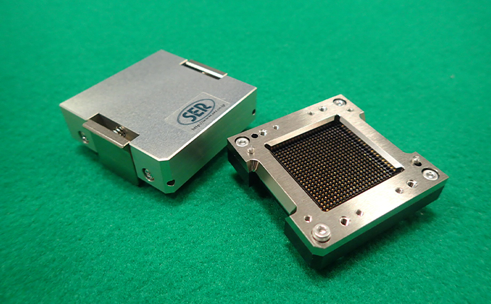
One touch cap
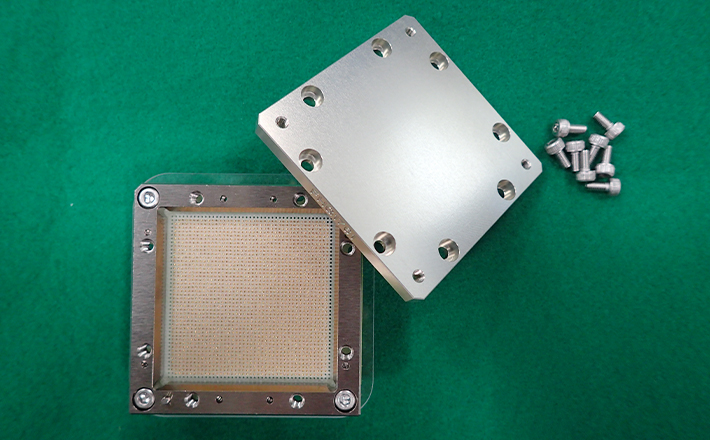
Screw cap
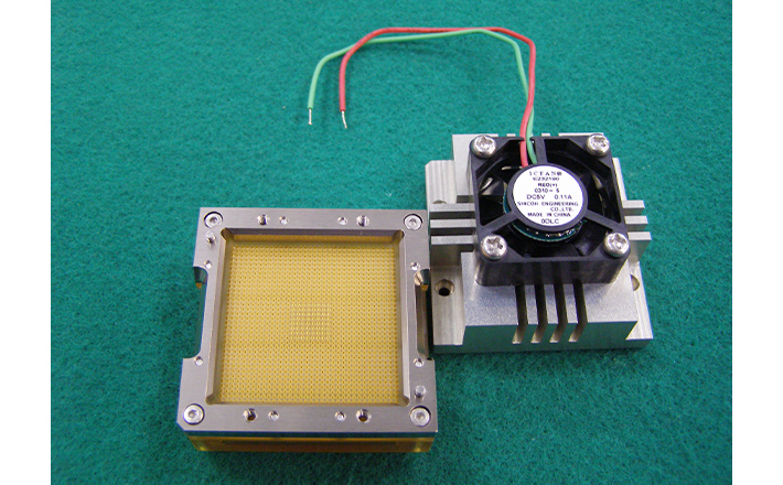
Heat sink & Fan type
Applications
1.FPGA/CPLD design and evaluation.
2.Field test, failure analysis and repair.
3.LSI and system verification and operating test.
4.ES test and final test.
2.Field test, failure analysis and repair.
3.LSI and system verification and operating test.
4.ES test and final test.
Socket size line up (Socket base)
Standard socket size for Pitch=1mm and Pitch=1.27mm as follows.
・Pitch=1mm:□39mm, □47mm, □60mm
・Pitch=1.27mm:□39mm, □47mm, □52mm, □60mm
Note1:It might be needed different size depend on package size and pin count.
Note2:Please contact if you need except the above pitch (ex Pitch=0.8mm).
・Pitch=1mm:□39mm, □47mm, □60mm
・Pitch=1.27mm:□39mm, □47mm, □52mm, □60mm
Note1:It might be needed different size depend on package size and pin count.
Note2:Please contact if you need except the above pitch (ex Pitch=0.8mm).
(Example)
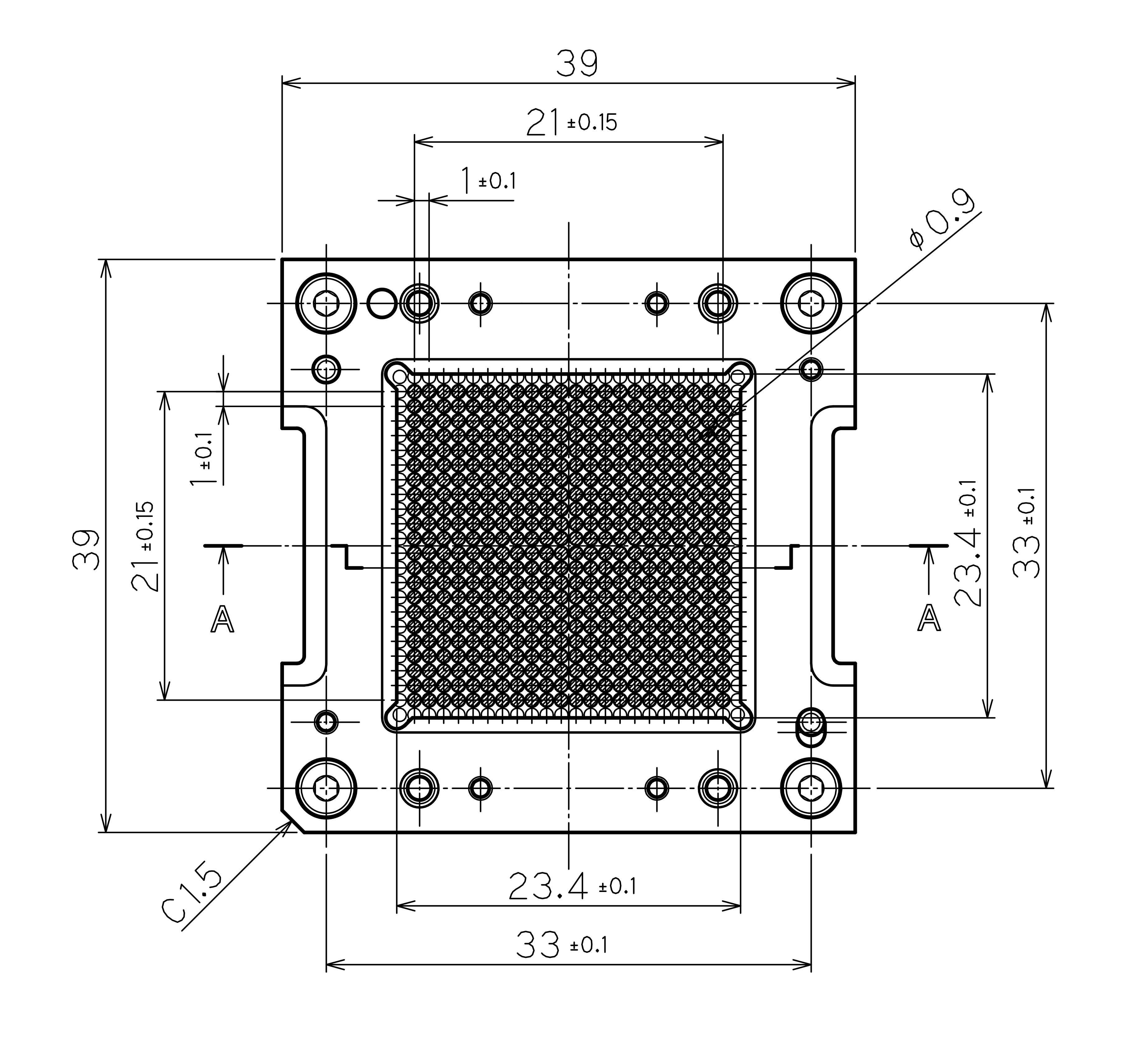
Socket base size=□39mm
・Pin count =484
・Pitch=1mm
・Package size=□23mm
Socket base size=□39mm
・Pin count =484
・Pitch=1mm
・Package size=□23mm
Important notice for PCB design
It is necessary to pay attention to design printed circuit board as follows.
1.Must PCB foot pattern same as IC matrix layout, and land size and circuit need compliant design rule for IC mounting.
2.Avoid making Through holes(TH) around pad center on the PCB.
3.Reccomend PCB thickness 1.6mm or thicker.
Recommend using support board under the PCB if the package has 676 pin or more, and PCB thickness is less than 1.6mm for considering pin count, probe force and PCB thickness.
(There might be a problem with PCB bowing if 500pin or 600pin count with PCB thickness is less than 1.6mm, or PCB thickness is 1.6mm with over 1000 pin count. )
4.Prohibit chip mount in the socket mounting area.
There is no special restriction with the back side of the PCB if it not use a support board except 4 Through holes(TH) which are used for mounting the socket.
However, if you would use the support board, chip mounting will be prohibited on the part of area.
Repair and Maintenance
It is possible to repair the solderless IC socket depending on the case such as tip wear, life-time and other damages.
In addition, the socket maintenance is useful for re-use and recover stable contact performance.
In addition, the socket maintenance is useful for re-use and recover stable contact performance.
1.Repair of the socket
It is easy replacement of the probe by user side because the socket has simple design. Also, we can sell spare parts for maintenance.
However, required careful and precise works, we can provide repair service if it difficult to handle on the user side.
However, required careful and precise works, we can provide repair service if it difficult to handle on the user side.
2.Cleaning and maintenance of the socket
If you would execute socket and probe cleaning with brush, the socket could significantly extend life-time.
The simple ways for cleaning are "Carefully brushing for a probe tip in the socket with toothbrush or brass brush", and "Air blow".
As the result, it is possible to remove contamination that might cause contact fail, and extend life-time.
The simple ways for cleaning are "Carefully brushing for a probe tip in the socket with toothbrush or brass brush", and "Air blow".
As the result, it is possible to remove contamination that might cause contact fail, and extend life-time.